
Advances in #Ga2O3 technology
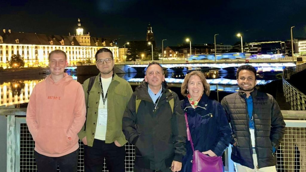
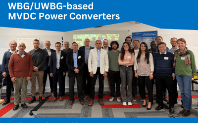
From September 22 to 24, members of the SAFEPOWER project team — Amador Perez Tomas (IMB-CNM-CSIC, Spain), Fernando-Pierre G. (IMB-CNM-CSIC, Spain), Aniol Vellvehí i Llovet (IMB-CNM-CSIC, Spain), Ekaterine Chikoidze (GEMaC, UVSQ – CNRS, France) and Edgars Butanovs (ISSP, Latvia) took part in the 8th International Workshop on Ultra-Wide Bandgap Materials and Devices (IWUMD2025), held in Wroclaw, Poland.
Amador Perez Tomas presented the work “𝗧𝘂𝗻𝗶𝗻𝗴 𝗦𝗶𝗹𝗶𝗰𝗼𝗻 𝗜𝗺𝗽𝗹𝗮𝗻𝘁𝗮𝘁𝗶𝗼𝗻 𝗳𝗼𝗿 α-𝗚𝗮₂𝗢₃ 𝗮𝗻𝗱 β-𝗚𝗮₂𝗢₃ 𝗠𝗘𝗦𝗙𝗘𝗧 𝗧𝗿𝗮𝗻𝘀𝗶𝘀𝘁𝗼𝗿𝘀”, coauthored by all the participated team members. Special mention for Edgars Butanovs (ISSP, Latvia) – the samples grower.
Main highlights:
- The article focuses on the development of Si-doped α-Ga₂O₃ layers using an ALD Al₂O₃ capping method.
- This technique allows high-temperature annealing compatible with β-Ga₂O₃ processing, aiming to activate doping efficiently in both phases
- The study addresses key aspects, including drift conductivity, Ohmic contact formation, and dopant activation, and highlights the potential of α-Ga₂O₃ for future high-voltage and UV optoelectronic devices.